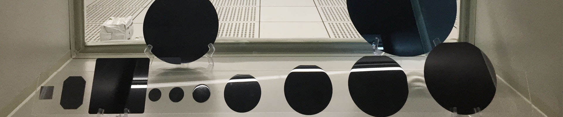
Epitaxial Layer is a thin film or layer structure formed on a substrate material by epitaxial growth technique.
Epitaxial layer technology is widely used in the fields of semiconductor, optoelectronics and materials science to prepare high-performance devices and materials.
Epitaxial layers can be classified according to their materials, growth methods and application areas.
The following are some common classifications of epitaxial layers:
According to the nature of the epitaxial layer classification
Homogeneous epitaxy: the epitaxial layer and the substrate are the same kind of material, for example, epitaxial growth of silicon on silicon, epitaxial growth of GaAs on GaAs belongs to homogeneous epitaxy.
Heterogeneous epitaxy: the substrate material and epitaxial layer are different materials, such as the epitaxial growth of silicon on sapphire, GaAlAs epitaxial growth on GaAs belongs to heterogeneous epitaxy.
Classification by device position
Positive epitaxial: the device is fabricated on the epitaxial layer.
Reverse epitaxial: the device is fabricated on the substrate, and the epitaxial layer only plays a supporting role.
Classified according to the epitaxial growth method
Direct Epitaxy: It is the method of heating, electron bombardment or applied electric field to make the growth of material atoms to obtain enough energy, direct migration and deposition on the substrate surface to complete the epitaxial growth method, such as vacuum deposition, sputtering, sublimation and so on. However, such methods are demanding on equipment. The resistivity of the film, the thickness of the repeatability is poor, so has not been able to be used in silicon epitaxial production.
Indirect Epitaxy: is the use of chemical reaction on the substrate surface deposition growth epitaxial layer, broadly known as chemical vapour deposition (chemical vapor deposition (CVD)). But the film grown by CVD is not necessarily a single crystal, so strictly speaking, only the growth of the film is a single crystal CVD is epitaxial growth. This method is simple equipment, epitaxial layer of various parameters easier to control, repeatability is good. Currently silicon epitaxial growth is mainly using this method.
Classified according to the method of transporting atoms
Vacuum Epitaxy: In ultra-high vacuum environment, molecular beam deposition (MBE) is used to deposit atoms or molecules of a material layer by layer on a substrate. MBE technology can achieve precise control of the atomic level and is widely used in the epitaxial growth of semiconductors and nanostructures.
Vapour Phase Epitaxy (VPE): A chemical reaction in the gas phase converts the precursors of a material into solid atoms and deposits them on a substrate to form an epitaxial layer; CVD is a common method for preparing epitaxial layers of semiconductors and ceramics.
Liquid Phase Epitaxy (LPE): During epitaxial layer growth, the solute material is dissolved in a solution, and then by controlling the saturation and temperature of the solution, the solute is deposited on the substrate to form an epitaxial layer.LPE technology is suitable for epitaxial growth of certain specific material systems, such as certain oxide and semiconductor materials.