What is silicon wafer polishing?
The significance of wafer polishing
Silicon processing, multi-wire cutting, grinding and other processing, will form a damage layer on the surface, thus making the surface has a certain roughness. Polishing is the process of further obtaining a smoother and flatter silicon single crystal surface through chemical-mechanical grinding methods on the basis of abrasive discs.
Abrasive roughness (before polishing): ~ 10-20um
Polishing disc roughness (after polishing): ~ tens of nm
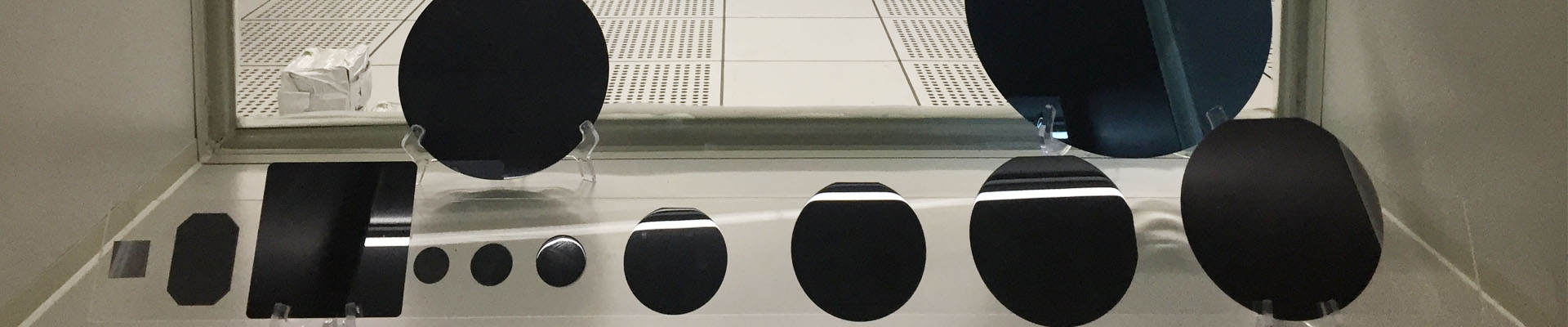
Abrasive wafers: thin wafers of a certain thickness, a body material, concerned only with certain characteristic parameters of the body, such as thickness, warpage, and parameters of the surface, such as chipping.
Polished wafers: silicon wafers with a smooth surface, mainly concerned with the characteristic parameters of the processed silicon surface.
Surface flatness of silicon polished wafers
Two parameters that describe flatness:
Total Indicated Reading (TIR): the difference between the highest and lowest points on the polished surface of the wafer, i.e. the peak-to-valley difference, which is positive only.
Focal Plane Deviation (FPD): the maximum value of the deviation from the reference plane between the two highest and lowest points of the surface, which can be positive or negative.
Chemical Mechanical Polishing (CMP)
The CMP process combines the advantages of both chemical and mechanical action to achieve very high surface flatness over a wide range, and is currently the only polishing technology that flattens the surface of large areas. Chemical-mechanical polishing with alkaline SiO2 is commonly used and can achieve roughness below 100 nm on 12 and 18 inch wafers.
During the CMP process, the alkali in the polishing solution reacts chemically with the silicon surface layer and produces a looser silicate (which adheres to the surface layer and impedes deeper reactions), which is then detached from the surface by the mechanical friction of the SiO2 gel particles and the polishing cloth pads, resulting in surface stripping. This process is repeated, thus stripping the silicon wafer layer by layer and achieving high precision polishing of the wafer.