Currently, glass wafers are mainly used in the following areas: MEMS and electronics, semiconductors, biotechnology and integrated circuit packaging.
MEMS and Electronics
MEMS and electronics use glass wafers for fabrication in wafer packaging and substrate carriers. In MEMS and electronics applications, glass wafers are used in wafer packaging of sensitive components because of their superior functionality and extreme reliability over time and in the face of harsh environments.
As a carrier substrate, glass is selected because of its thermal stability and chemical resistance. In the medical device industry, these wafers are used to promote airtight MEMS enclosures.
Semiconductors
Glass wafers are used as carrier substrates in the production of semiconductor wafers, which are made of finer materials that are easily bent or torn. Glass substrate components can safely handle semiconductor wafers, despite their fine and thin texture. Glass was chosen because of its superior chemical and thermal stability, and the potential for reuse to reduce the cost and environmental impact of some applications.
Biotechnology
Glass wafers used in a variety glass substrate of biotechnology applications. Borosilicate glass is a premium choice in medical device glass because of its excellent resistance to high temperature and energy as well as radiation exposure, for example in X-ray equipment.
Wafers are also used to produce microfluidic chips by using nanoimprint lithography, in which glass acts as the substrate. Glass provides the clear optical transparency required for many biotechnology applications, making it a common choice for using as overlays on devices of silicon. Wafer bonding processes, such as anode bonding and thermal bonding, create air-tight seal.
Integrated Circuit
Glass wafers are used in a variety of integrated circuit (IC) packaging applications, providing better performance and cost effectiveness as substrates. Glass through-holes (TGVS) and wafer-grade glass caps (WLC) are improved packaging solutions that offer enhanced technical performance, this is thanks to specific glass characteristics, including stiffness and roughness below 0.5 nm rms. Glass protects the IC from shock and corrosion while maintaining the pins and leads that connect to the external circuit.
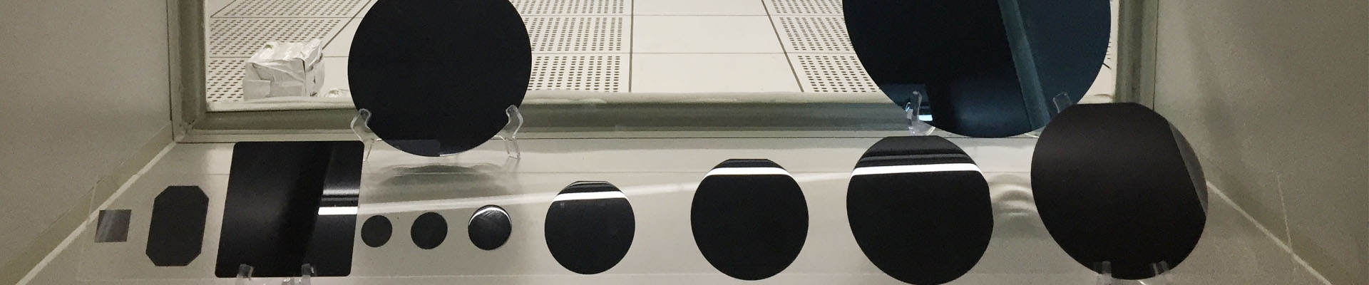
Technical Specifications
| Diameter |
2inch |
3inch |
4inch |
5inch |
6inch |
8inch |
12inch |
| Thickness (um) |
Depends on Request |
| Material |
Fused Silica、Quartz、Single Crystal、Soda Lime、K9Glass、Schott Glass、Corning Glass |
| Grade/Brand |
JGS1、JGS2、JGS3、Single Crystal、Soda Lime、K9、B270i、BOROFLOAT33、D263t、N-BK7、7980、Eagle-XG、sapphire 、Zerodur、SK-1300 |
| Surface Finished |
DSP、SSP、DSL |
| TTV (um) |
<5 |
<5 |
<5 |
<5 |
<5 |
<10 |
<15 |
| Bow/Warp (um) |
<20 |
<20 |
<30 |
<30 |
<30 |
<40 |
<60 |
| Ra (nm) |
<1 |
| S/D (um) |
40/20 |
special indexes:
Ultra-flat glass wafer: TTV<1um
Ultra-thin glass wafer: Thickness:0.1-0.3um
Ultra-smooth glass wafer: Ra≤0.2nm
|