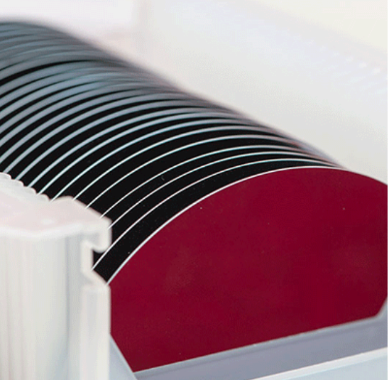
| Diameter |
2" |
3" |
4" |
5" |
6" |
8" |
| Growth Method |
FZ |
| Orientation |
< 1-0-0 > , < 1-1-1 > |
| Type/Dopant |
Intrinsic, N Type/Phos, P Type/Boron |
| Thickness (um) |
279 |
380 |
525 |
625 |
675 |
725 |
| Thickness Tolerance |
Standard ± 25um |
±50um |
| Resistivity(Ω•cm) |
1000-20000, Maximum Capabilities>20000, and 1-5 |
| Surface Finished |
P/E , P/P, E/E, G/G |
| TTV (um) |
Standard < 10 um |
| Bow/Warp (um) |
Standard <40 um |
<50um |
| Particle |
<10@0.3um |
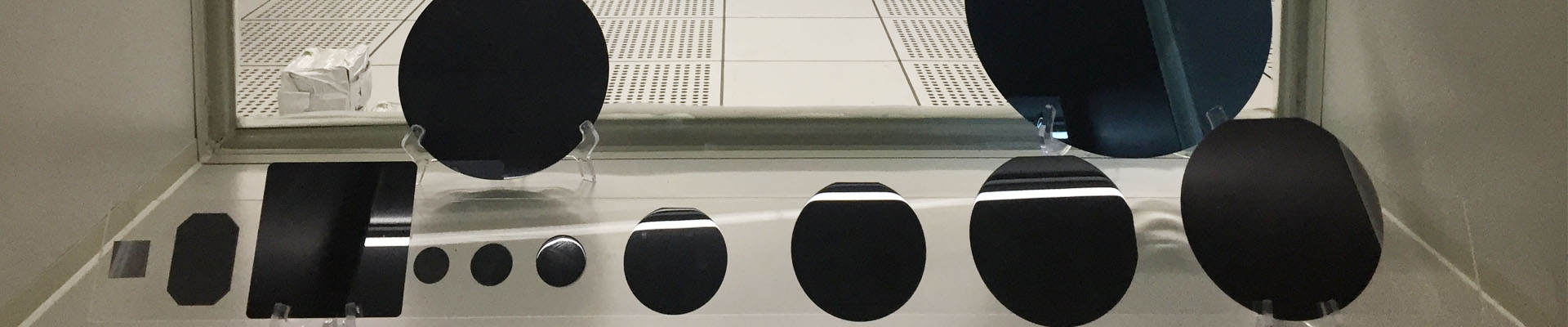
Float Zone Silicon
The Float Zone (FZ) Method produces a highly pure form of silicon.
The purity of the material allows for lower defect concentrations and higher resistivity levels and it is useful in high-power devices, detectors and solar applications.
PLUTO offers the very best Float Zone material commercially available, not made from CZ re- melts but from high-quality polysilicon, thus allowing for resistivity’s in excess of 10k ohm–cm.
PLUTO is the exclusive China distributor, bringing world-class Float Zone silicon to the world market since 2010.
Available in various specifications and Diameters up to 200mm.
Neutron Transmutation Doped (NTD) Float Zone silicon:
The lowest resistivity variation of any crystalline silicon product on the market. NTD silicon products in the widest range of resistivities ranging from 5 Ω•cm to 4000 Ω•cm.