
The diameter and thickness of wafers are two core parameters, which not only reflect the technological progress of the industry, but also directly related to the efficiency and cost of chip production. With the continuous progress of science and technology, we have witnessed the evolution from small-sized wafers to large-sized wafers, and the changes in wafer thickness during this process have also attracted extensive attention from the industry. This article will explore the relationship between wafer diameter and thickness, and how they affect the development of the semiconductor industry.
Evolution of Wafer Diameter
Future Prospects
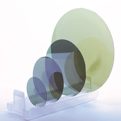
The diameter of semiconductor wafers has gradually grown from 50 (about 2 inches) in the early days to 300mm (about 12 inches) today, and is even moving towards 450mm (about 18 inches). Each increase in diameter means that more chips can be cut from a single wafer, thereby increasing production efficiency and reducing the cost of a single chip.
Thickness Adjustments and Challenges
As the diameter increases, the thickness of the wafer is adjusted accordingly. This is because larger wafers require better mechanical stability during fabrication and handling to prevent breakage or bending during transportation or manufacturing. For example, the standard thickness of a 200mm wafer is approximately 725μm, while the thickness of a 300mm wafer increases to approximately 775μm.
While increased thickness improves wafer stability, it also brings new challenges, such as thermal management issues and increased processing difficulty. Thicker wafers mean that heat may be distributed more unevenly during the fabrication process, which may affect the quality of the chips fabricated on the wafer.
Technological Advances Drive Change
To address these challenges, new technologies are constantly being developed in the industry. For example, by improving the wafer preparation process and adopting more advanced materials, it is possible to moderately control the thickness of a wafer without sacrificing its stability. In addition, with advances in wafer flattening technology, even larger-sized wafers can maintain good flatness, further improving the precision and quality of chip manufacturing.
Looking ahead, with the gradual maturation of 450mm wafer technology, we can foresee that the thickness adjustment of larger size wafers will be one of the focuses of industry research. At the same time, with the application of new materials, new processes, how to ensure the mechanical stability of the wafer at the same time, optimize its thickness to adapt to the needs of high-efficiency, low-cost production, will be an important challenge for the semiconductor industry.
Conclusion
The optimization of wafer diameter and thickness is an important symbol of technological progress in semiconductor manufacturing. As technology continues to evolve, the semiconductor industry will continue to explore more efficient and lower cost production methods. An in-depth understanding of the relationship between wafer diameter and thickness will help us better grasp the pulse of industry development and embrace the future of semiconductor technology.