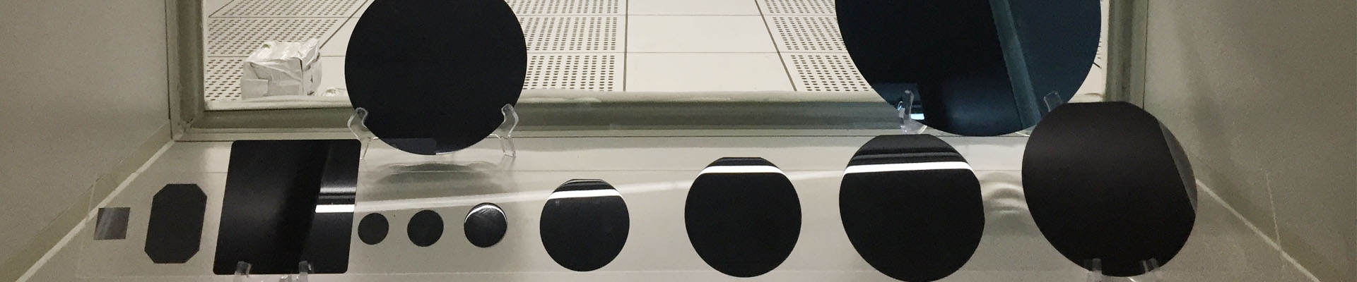
First, let’s introduce a basic concept: wafer fabrication includes two main processes, substrate preparation and epitaxial growth.
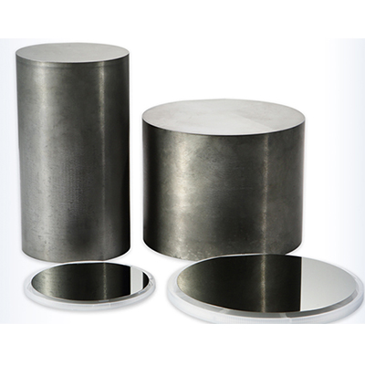
A substrate is a wafer made from a semiconductor single crystal material. The substrate can directly enter the wafer manufacturing process to produce semiconductor devices, or it can undergo epitaxial processing to produce an epitaxial wafer.
Epitaxy refers to the process of growing a new single crystal layer on a carefully cut, ground, and polished single crystal substrate. The new single crystal can be the same material as the substrate or a different material (homogeneous epitaxy or heterogeneous epitaxy).
Since the newly grown single crystal layer extends and grows following the crystal phase of the substrate, it is called an epitaxial layer (the thickness is usually a few micrometers, for example, in silicon: the significance of silicon epitaxial growth is to grow a layer on a silicon single crystal substrate with a certain crystal orientation that has the same crystal orientation as the substrate but different resistivity and thickness, and good lattice structure integrity), and the substrate with the grown epitaxial layer is called an epitaxial wafer (epitaxial wafer = epitaxial layer + substrate).
Device fabrication on the epitaxial layer is called epitaxy, while if device fabrication is on the substrate, it is called reverse epitaxy; in this case, the epitaxial layer only serves a supporting role.
Homogeneous epitaxy & Heterogeneous epitaxy
| Homogeneous epitaxy: |
Epitaxial layer of the same material as the substrate: e.g.Si/Si、GaAs/GaAs、GaP/GaP; |
| Heterogeneous epitaxy |
The epitaxial layer is not of the same material as the substrate: e.g.Si/Al2O3、GaS/Si、GaAlAs/GaAs、GaN/SiC and so on. |
Methods of Epitaxial Growth
Molecular Beam Epitaxy (MBE): MBE is a semiconductor epitaxial growth technique performed under ultra-high vacuum conditions. In this technique, source materials are evaporated in the form of atomic or molecular beams and then deposited on the crystal substrate. MBE is a highly precise and controllable semiconductor thin film growth technique that allows for atomic-level precision in controlling the thickness of the deposited material.
Metal-Organic Chemical Vapor Deposition (MOCVD): In the MOCVD process, organometallic and hydride gases containing the required elements are supplied to the substrate at appropriate temperatures. A chemical reaction occurs to produce the desired semiconductor material, which is deposited on the substrate, while the remaining compounds and reaction products are expelled.
Vapor Phase Epitaxy (VPE): Vapor phase epitaxy is an important technology commonly used in the production of semiconductor devices. Its basic principle involves transporting the vapor of an element or compound in a carrier gas, which then undergoes a chemical reaction to deposit a crystal on the substrate.